


Ask For A Quick Quote
We will contact you within one working day. Please pay attention to your email.
Request a Sample
With the mission of “Smart Manufacturing - Global Delivery”, we help our customers shorten the time-to-market and optimize the supply chain cost through continuous technology iteration and digital upgrading. We look forward to working with you to define the future of electronic manufacturing!
- Technology Driven Intelligent Manufacturing
- Full-process quality control
- In-depth industry experience
- Agile Service Network

Educational Equipment PCB Assembly
One-stop PCBA/EMS Intelligent Manufacturing Solution


Educational Equipment PCB Assembly
The Role of PCBs in Educational Equipment
Printed Circuit Boards (PCBs) form the foundational technology in educational equipment, enabling interactive learning tools, digital devices, and laboratory instruments to function efficiently and reliably. By providing a compact, organized platform for electrical connections and component integration, PCBs support the delivery of consistent performance and user-friendly interfaces essential for educational settings.
1. Enabling Interactive and Digital Learning
PCBs integrate microcontrollers, sensors, and display modules that power interactive devices such as tablets, electronic whiteboards, and learning kits.
They facilitate real-time feedback, multimedia content delivery, and adaptive learning experiences.
2. Supporting Laboratory and Experimental Instruments
In educational labs, PCBs provide the backbone for measurement, control, and data acquisition systems, ensuring accuracy and repeatability in experiments.
Robust PCB designs allow for reliable operation despite frequent handling and diverse environmental conditions.
3. Facilitating Connectivity and Communication
PCBs enable wired and wireless connectivity modules, allowing educational devices to connect to networks, share data, and integrate with learning management systems.
4. Enhancing Durability and Safety
Educational equipment PCBs are designed to meet strict safety standards and incorporate protective features to ensure safe use by students.
Durable materials and coatings help devices withstand frequent use and handling.
5. Allowing Cost-Effective Mass Production
The standardized manufacturing of PCBs helps keep educational equipment affordable while maintaining quality and performance across large volumes.
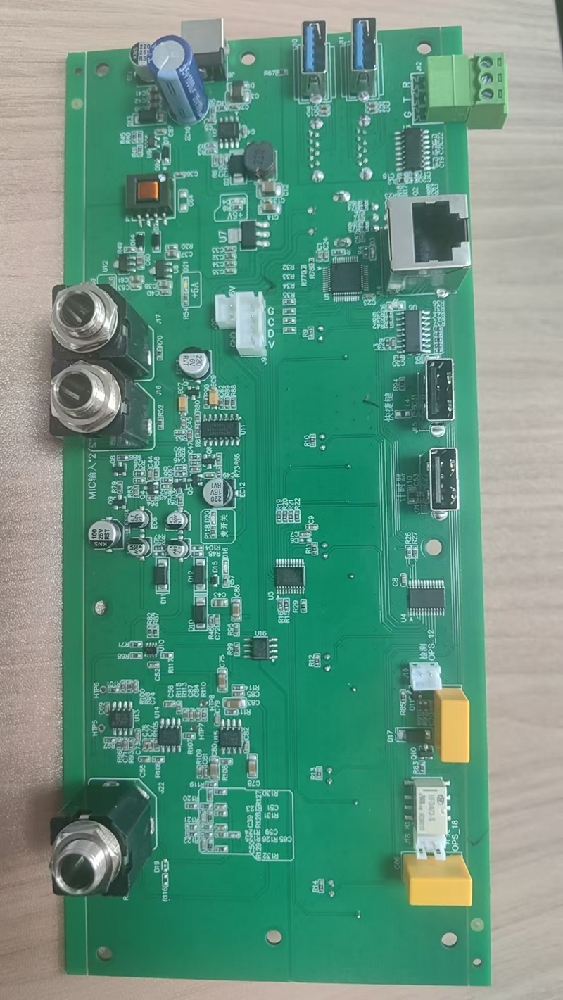
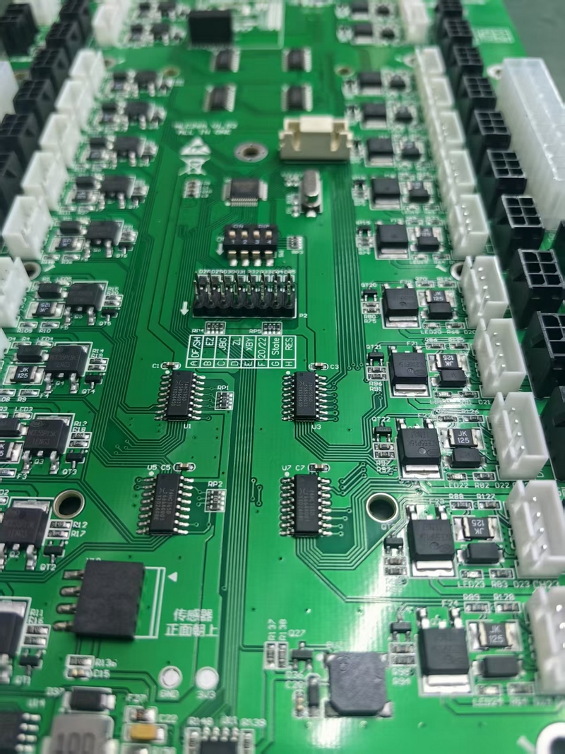
Key Components of Educational Equipment PCB Assembly
Here are the Key Components of Educational Equipment PCB Assembly:
1.Microcontrollers and Microprocessors – Act as the central brain to process inputs, execute instructions, and control output devices in educational tools.
2.Sensors – Include temperature, motion, light, or sound sensors for interactive and responsive learning experiences.
3.Memory Modules – Store programs, instructional content, and collected data for offline and online educational applications.
4.Display Modules – LCD, LED, or touchscreen interfaces for visualizing educational content and user interaction.
5.Connectivity Modules – Wi-Fi, Bluetooth, or Ethernet components for connecting devices to the internet, school networks, or cloud platforms.
6.Power Supply Components – Voltage regulators, batteries, and power management circuits to ensure stable operation in various environments.
7.Audio Components – Speakers, microphones, and amplifiers for delivering and recording sound in language labs, e-learning devices, or multimedia equipment.
8.Interface Ports – USB, HDMI, or GPIO connectors for expansion, peripheral devices, and interactive hardware integration.
9.Protection Components – Fuses, ESD protection, and surge suppression to safeguard delicate electronics from damage.
10.Embedded Software Integration Points – Firmware-supporting chips and components that enable programmable, adaptable educational solutions.
Materials and Technologies for Educational Equipment PCB Assembly
Educational equipment often combines reliability, durability, and cost-effectiveness, requiring PCB assemblies that can withstand frequent handling, varying environments, and long-term usage. The materials and technologies selected must balance performance with affordability while meeting safety and compliance standards.
1. PCB Substrate Materials
FR-4 Epoxy Glass Laminate – The most common choice for educational devices due to its affordability, electrical insulation, and mechanical strength.
High-Tg FR-4 – Offers better thermal stability for equipment that may generate more heat, such as lab measurement tools or interactive boards.
Flexible Polyimide Substrates – Used in foldable, portable, or space-saving devices like handheld learning tools.
Aluminum-Core PCBs – Beneficial in educational equipment with high-power LEDs (e.g., lab lighting systems, visual display boards).
2. Conductive Materials
Copper Foil – Standard for creating conductive traces, with thickness varying based on current requirements.
Silver Ink – Used in printed electronics for low-cost, low-power applications like smart training aids.
3. Surface Finishes
HASL (Hot Air Solder Leveling) – Cost-effective for general applications where ultra-fine pitch is not critical.
ENIG (Electroless Nickel Immersion Gold) – Provides excellent solderability and flatness, ideal for precise educational tools like microscopes or measurement devices.
OSP (Organic Solderability Preservative) – Eco-friendly and suitable for lead-free assembly in compliance with RoHS standards.
4. Assembly Technologies
SMT (Surface Mount Technology) – Enables compact, lightweight designs for portable educational devices.
THT (Through-Hole Technology) – Used for connectors, mechanical stability, and components that require high durability.
Hybrid Assembly – Combines SMT and THT to achieve both miniaturization and robustness.
Automated Optical Inspection (AOI) – Ensures high assembly quality, reducing field failures in educational environments.
5. Special Design Considerations
ESD Protection – For devices used in lab experiments or environments with sensitive electronics.
Durability Enhancements – Conformal coating or potting to protect against moisture, dust, and rough handling.
Low-Power Optimization – Essential for battery-operated educational equipment to extend usage time.
Educational Equipment PCB Assembly Process
The assembly process for PCBs used in educational equipment demands a balance between cost-effectiveness, durability, and functionality to ensure long-term reliability in learning environments. Below is a step-by-step overview:
1. Design & Prototyping
Schematic & PCB Layout: Engineers design the circuit based on the device’s learning functions, ensuring safety compliance for student use.
Prototype Fabrication: Initial prototypes are produced to validate performance, ergonomics, and user-friendliness.
2. Material Preparation
Substrate Cutting: FR-4 or alternative eco-friendly materials are cut to precise dimensions.
Surface Cleaning: Boards are cleaned to remove dust, oils, and contaminants to ensure optimal soldering.
3. Component Placement (SMT & Through-Hole)
SMT Assembly: Automated pick-and-place machines position resistors, capacitors, microcontrollers, and display modules.
Through-Hole Assembly: Components like connectors, mechanical switches, and power modules are inserted manually or semi-automatically.
4. Soldering Process
Reflow Soldering: Used for SMT components, with controlled heating profiles to prevent thermal damage.
Wave or Selective Soldering: For through-hole components, ensuring strong mechanical and electrical joints.
5. Inspection & Testing
AOI (Automated Optical Inspection): Detects soldering defects, component misalignment, or missing parts.
Functional Testing: Ensures the board meets educational equipment requirements, such as interactive response speed or sensor accuracy.
6. Conformal Coating (Optional)
Adds a protective layer to guard against moisture, dust, and accidental spills in classroom environments.
7. Final Assembly & Packaging
Boards are integrated into casings, labeled, and packaged for safe transport to educational institutions.
Future Implications of Educational Equipment PCB Assembly
As educational technology continues to advance, PCB assembly for educational equipment is expected to play an increasingly pivotal role in transforming learning environments. Several trends and innovations are set to shape the future:
1,Integration of Smart and Interactive Technologies
The growing adoption of AR/VR systems, AI-driven tutoring tools, and IoT-enabled classroom devices will demand highly specialized PCB designs with increased processing power, wireless capabilities, and sensor integration.
2,Miniaturization and Portability
Portable and modular learning devices will require compact, lightweight PCBs with flexible designs, enabling students to learn anytime and anywhere without sacrificing functionality.
3,Enhanced Connectivity
The rise of cloud-based education and remote learning platforms will push for PCBs with robust wireless modules (Wi-Fi 6, Bluetooth 5.3, 5G), ensuring fast and stable communication between devices and learning platforms.
4,Sustainability and Eco-Friendly Designs
With environmental awareness becoming a priority, educational institutions will increasingly prefer PCBs made from lead-free materials, recyclable substrates, and energy-efficient components.
5,Customizable and Adaptive Hardware
Future educational PCBs will likely feature modular architectures, allowing institutions to adapt or upgrade hardware for different courses, levels, or technologies without replacing entire systems.
6,Improved Reliability and Longevity
As educational budgets tighten, demand for PCBs with extended lifespans, low maintenance requirements, and strong resistance to wear and tear will grow.
In short, the future of educational equipment PCB assembly will be characterized by smarter, greener, and more adaptable designs, directly influencing the way students learn and teachers teach.
Conclusion
Educational equipment PCB assembly plays a critical role in enabling innovative, reliable, and interactive learning technologies. By integrating advanced design techniques, durable materials, and precise manufacturing processes, these PCBs support the high performance, safety, and longevity required in educational environments. As education continues to embrace digital transformation—through tools like interactive whiteboards, virtual labs, and AI-powered learning devices—the demand for robust, scalable, and energy-efficient PCB solutions will only increase. Companies that invest in cutting-edge PCB assembly capabilities today will be better positioned to meet the growing needs of future-ready educational systems.
Ready to Elevate Your PCB Projects to New Heights?
Whether you’re developing advanced educational tools, high-speed communication systems, or cutting-edge IoT devices, the right PCB assembly partner can make all the difference. By combining expertise, precision manufacturing, and a commitment to innovation, we deliver PCB solutions that meet your performance, reliability, and scalability needs. Let’s work together to transform your ideas into powerful, future-ready products that inspire learning and drive progress.
Request A Quote
Please feel free to contact us at any time, and we will wholeheartedly provide you with the highest quality service and support.