




Ask For A Quick Quote
We will contact you within one working day. Please pay attention to your email.
Request a Sample
With the mission of “Smart Manufacturing - Global Delivery”, we help our customers shorten the time-to-market and optimize the supply chain cost through continuous technology iteration and digital upgrading. We look forward to working with you to define the future of electronic manufacturing!
- Technology Driven Intelligent Manufacturing
- Full-process quality control
- In-depth industry experience
- Agile Service Network
Exploring the Intersection of Communication, AIoT, and PCB Assembly
2026-08-15
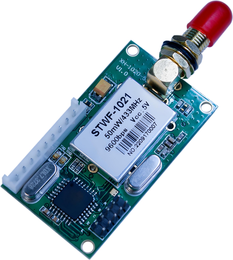
In today's rapidly evolving technological landscape, the integration of communication technologies and AIoT with PCB assembly plays a pivotal role in the development of advanced electronic devices. Communication is the backbone of connectivity, enabling devices to interact seamlessly within an ever-expanding network of interconnected systems. AIoT, which refers to the convergence of artificial intelligence and the Internet of Things, enhances this connectivity by empowering devices with intelligent capabilities, allowing them to analyze data, make decisions, and optimize performance autonomously.
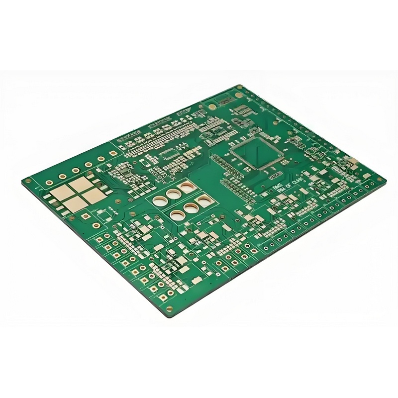
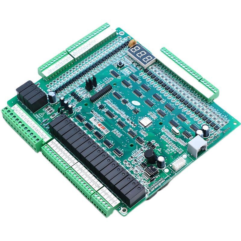
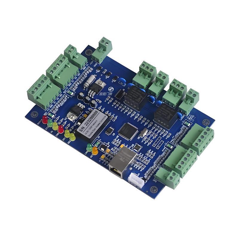
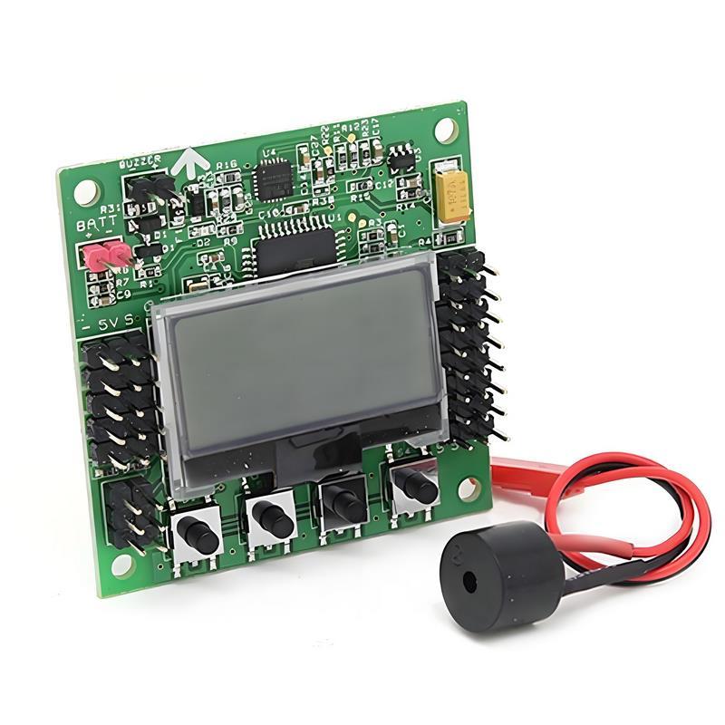
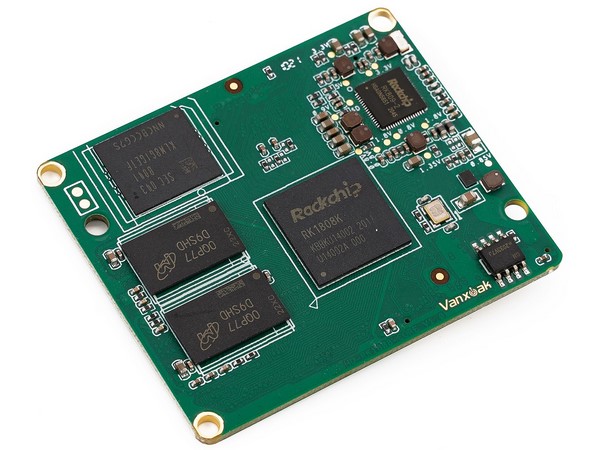
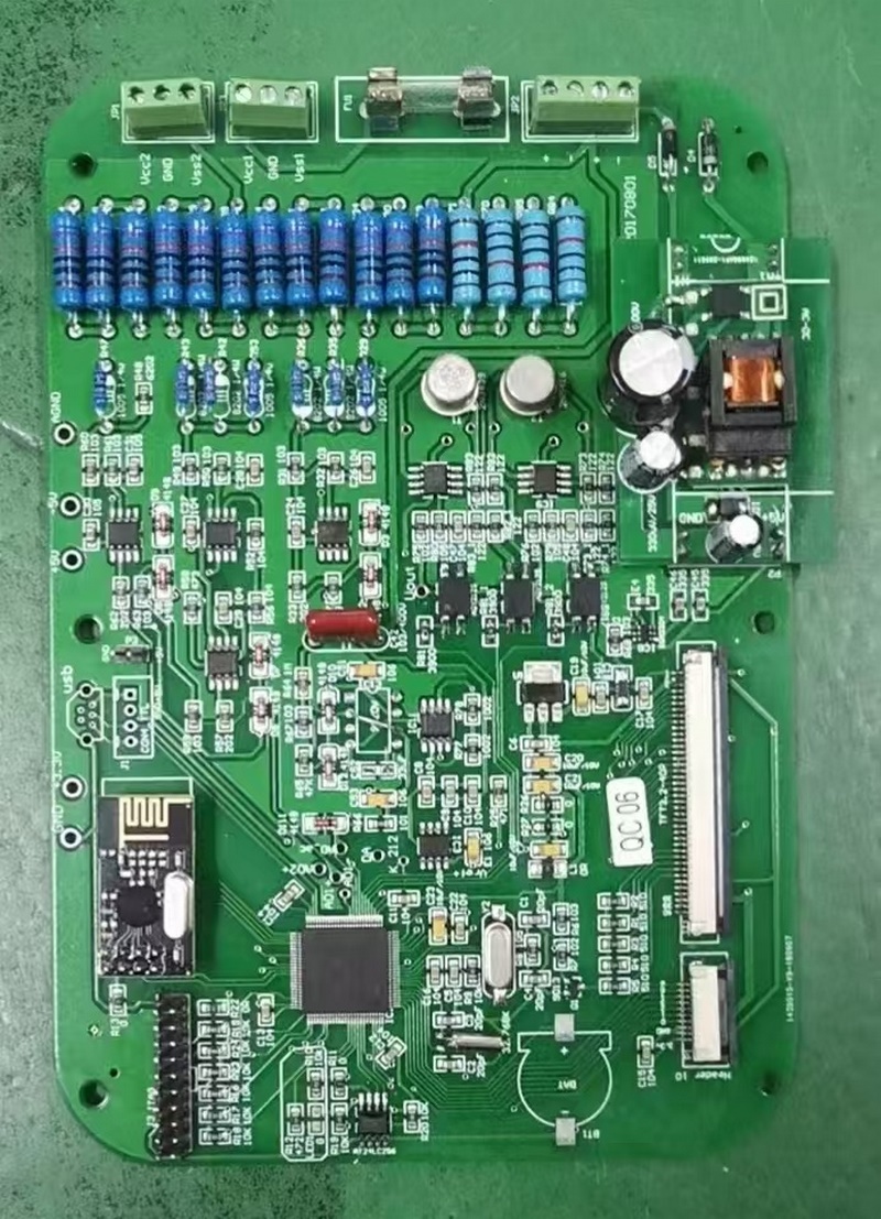
Printed Circuit Board Assembly (PCB Assembly) is a crucial aspect of electronic manufacturing. It involves the process of soldering electronic components onto a PCB, which serves as the foundation for electronic circuits. As devices become smarter and more connected, the demand for high-quality, efficient PCB assembly has surged. The synergy between communication technologies and AIoT necessitates that PCBs are designed with precision and reliability to accommodate complex functionalities and high-performance standards.
One significant trend in communication and AIoT PCB assembly is the miniaturization of components. As devices shrink in size, the PCB must also adapt, requiring sophisticated design techniques to fit more functionalities into a compact form. This miniaturization is not only about saving space but also about improving performance and energy efficiency. Smaller components can lead to faster signal transmission and reduced power consumption, which are critical factors in the design of modern electronic devices.
Furthermore, the incorporation of AI in PCB design and assembly processes is revolutionizing how manufacturers approach production. AI algorithms can predict potential issues in the manufacturing process, such as defects or inefficiencies, thereby significantly reducing waste and enhancing quality control. This predictive capability is essential for companies striving to meet the increasing demand for reliable and efficient electronic components.
Another important aspect of communication and AIoT PCB assembly is the need for robust security protocols. As devices become more interconnected, they also become more vulnerable to hacking and cyber threats. Ensuring that PCBs are designed with security in mind is paramount to protect sensitive data and maintain user trust. Security features might include encryption-enabled chips or secure boot mechanisms, which can safeguard devices against unauthorized access.
In summary, the intersection of communication technologies, AIoT, and PCB assembly is a dynamic and rapidly evolving field. As the demand for smarter, more connected devices continues to grow, understanding the intricacies of this relationship will be essential for professionals in the electronics industry. By leveraging advancements in AI and ensuring high-quality PCB assembly, manufacturers can position themselves at the forefront of innovation in electronic components.
Printed Circuit Board Assembly (PCB Assembly) is a crucial aspect of electronic manufacturing. It involves the process of soldering electronic components onto a PCB, which serves as the foundation for electronic circuits. As devices become smarter and more connected, the demand for high-quality, efficient PCB assembly has surged. The synergy between communication technologies and AIoT necessitates that PCBs are designed with precision and reliability to accommodate complex functionalities and high-performance standards.
One significant trend in communication and AIoT PCB assembly is the miniaturization of components. As devices shrink in size, the PCB must also adapt, requiring sophisticated design techniques to fit more functionalities into a compact form. This miniaturization is not only about saving space but also about improving performance and energy efficiency. Smaller components can lead to faster signal transmission and reduced power consumption, which are critical factors in the design of modern electronic devices.
Furthermore, the incorporation of AI in PCB design and assembly processes is revolutionizing how manufacturers approach production. AI algorithms can predict potential issues in the manufacturing process, such as defects or inefficiencies, thereby significantly reducing waste and enhancing quality control. This predictive capability is essential for companies striving to meet the increasing demand for reliable and efficient electronic components.
Another important aspect of communication and AIoT PCB assembly is the need for robust security protocols. As devices become more interconnected, they also become more vulnerable to hacking and cyber threats. Ensuring that PCBs are designed with security in mind is paramount to protect sensitive data and maintain user trust. Security features might include encryption-enabled chips or secure boot mechanisms, which can safeguard devices against unauthorized access.
In summary, the intersection of communication technologies, AIoT, and PCB assembly is a dynamic and rapidly evolving field. As the demand for smarter, more connected devices continues to grow, understanding the intricacies of this relationship will be essential for professionals in the electronics industry. By leveraging advancements in AI and ensuring high-quality PCB assembly, manufacturers can position themselves at the forefront of innovation in electronic components.
Related news

Request A Quote
Please feel free to contact us at any time, and we will wholeheartedly provide you with the highest quality service and support.