




Ask For A Quick Quote
We will contact you within one working day. Please pay attention to your email.
Request a Sample
With the mission of “Smart Manufacturing - Global Delivery”, we help our customers shorten the time-to-market and optimize the supply chain cost through continuous technology iteration and digital upgrading. We look forward to working with you to define the future of electronic manufacturing!
- Technology Driven Intelligent Manufacturing
- Full-process quality control
- In-depth industry experience
- Agile Service Network
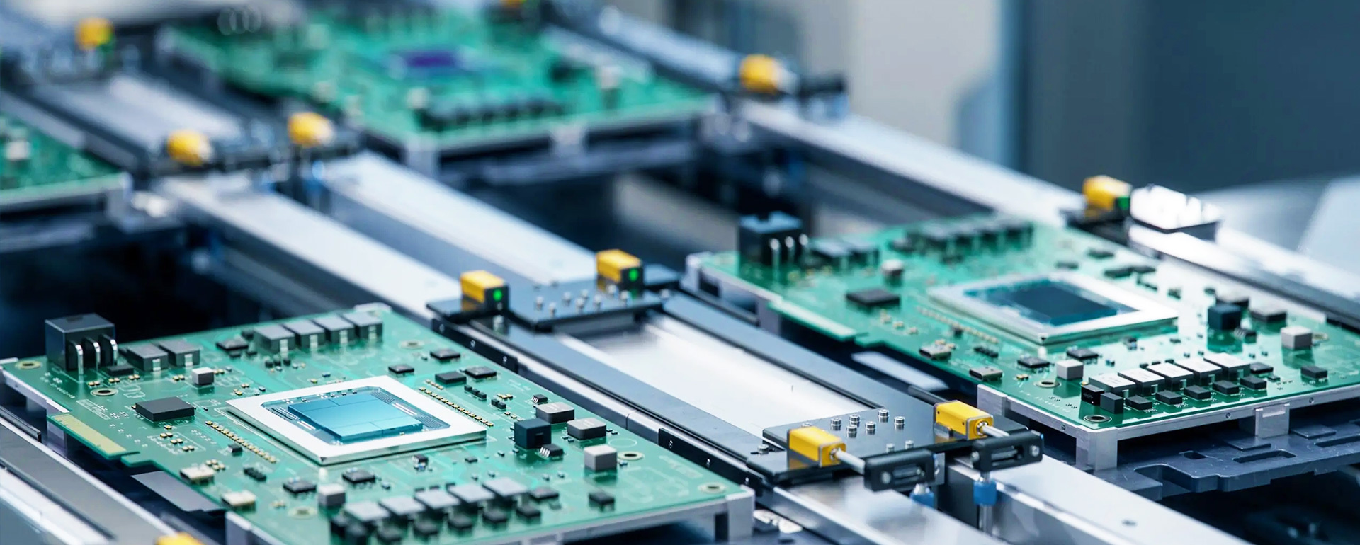
PCB Assembly
One-stop PCBA/EMS Intelligent Manufacturing Solution
Communication and AIoT Assembly
Introduction
Welcome to the interconnected world of communication and AIoT PCB assembly, which refers to the production and assembly of printed circuit boards used in communication devices and AIoT applications. These assemblies require high precision, reliability, and signal integrity to support functions such as data transmission, wireless connectivity, edge computing, and intelligent control.
We offer one-stop PCBA solutions for communication modules (e.g., 4G/5G, Wi-Fi, Bluetooth), smart gateways, IoT terminals, and AI-integrated devices. With advanced SMT lines, strict quality control, and support for high-frequency, multi-layer PCB designs, we ensure consistent performance and fast time-to-market for our customers in the rapidly evolving communication and AIoT sectors.
Our services include PCB fabrication, component sourcing, assembly, testing, and complete system integration, tailored to meet the diverse requirements of smart connected products.
Understanding Communication and AIoT Assembly PCBs
Communication and AIoT Assembly PCBs are specialized printed circuit boards designed for devices that require wireless connectivity, data processing, and intelligent control. These PCBs are the backbone of modern smart systems such as routers, gateways, 5G modules, edge computing devices, smart meters, and AI-based sensors.
They often involve high-speed signal transmission, RF design, multi-layer structures, and integration of complex components like microcontrollers, AI chips, and wireless modules (e.g., Wi-Fi, Bluetooth, NB-IoT, LoRa). Assembly of such boards demands high-precision SMT technology, rigorous testing (ICT/FCT/AXI), and strong EMC (Electromagnetic Compatibility) control.
In the PCBA industry, manufacturers must not only ensure quality soldering and accurate component placement but also focus on thermal management, signal integrity, and long-term reliability—key factors for success in communication and AIoT products.
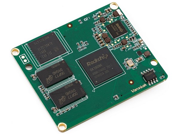
Essential Components of Communication and AIoT PCB Assembly
|
Component |
Function / Description |
|
Microcontrollers / MCUs |
Control system logic, data processing, and peripheral communication |
|
Wireless Modules |
Provide wireless connectivity (Wi-Fi, Bluetooth, LoRa, NB-IoT, LTE, 5G, etc.) |
|
AI Chips / NPUs |
Handle machine learning tasks and intelligent decision-making |
|
RF Components |
Include antennas, filters, and RF ICs for signal transmission and reception |
|
Memory Chips |
Store firmware, operational data, and logs (e.g., Flash, EEPROM, RAM) |
|
Sensors |
Collect environmental or user data (e.g., temperature, motion, pressure) |
|
Power Management ICs (PMICs) |
Manage and distribute power efficiently across the board |
|
Connectors & Interfaces |
Enable communication with external devices (USB, UART, I2C, SPI, Ethernet, SIM, etc.) |
|
Crystal Oscillators |
Generate precise timing signals for system synchronization |
|
Passive Components |
Resistors, capacitors, inductors – essential for filtering, stability, and signal shaping |
|
Protection Components |
TVS diodes, ESD protectors, and fuses to prevent electrical damage |
|
PCB Substrate & Stack-Up |
Multi-layer materials (e.g., FR4, Rogers) for signal integrity and high-speed design |
Best Practices for communication and AIoT PCB Assembly
| Category | Best Practice |
| Design & Layout |
- Use controlled impedance routing for high-speed and RF signals - Minimize EMI by using proper grounding, shielding, and layer stack-up -Follow design-for-manufacturing (DFM) and design-for-test (DFT) guidelines - Place sensitive analog and RF components away from noisy digital circuits - Keep antenna areas clear of ground planes and traces |
| Component Selection |
-Choose high-reliability components rated for IoT/industrial environments -Verify compatibility and communication protocols (I2C, UART, SPI, etc.) - Use certified wireless modules for faster compliance and integration |
| Assembly Process |
-Employ high-precision SMT machines for tight-pitch and miniaturized components -Use proper solder paste for fine-pitch, high-density interconnects (HDI) -Handle moisture-sensitive devices (MSDs) under appropriate MSL conditions -Conduct X-ray inspection for BGA and hidden solder joints |
| Testing & Validation |
-Implement ICT (In-Circuit Testing) and FCT (Functional Circuit Testing) - Perform RF testing for signal strength, interference, and modulation accuracy - Run environmental and thermal tests for reliability in various operating conditions -Ensure software/firmware is tested in real hardware conditions (burn-in, stress tests) |
| Compliance & Reliability |
-Design with certification in mind (CE, FCC, RoHS, etc.) - Plan for ESD protection and surge suppression -Focus on long-term supply chain stability for critical parts |
Advanced Technologies and Innovations in Communication and AIoT PCB Assembly
As the demand for intelligent connectivity and real-time data processing continues to grow, the assembly of communication and AIoT (Artificial Intelligence of Things) PCBs has rapidly evolved to incorporate cutting-edge technologies and innovative manufacturing techniques. These advancements enable the production of smaller, faster, and more reliable smart devices that support 5G communication, edge computing, and AI-driven applications. From high-density interconnect (HDI) and flexible PCBs to AI-assisted testing and advanced material usage, manufacturers are leveraging a range of new solutions to meet the stringent performance, reliability, and environmental requirements of next-generation communication and AIoT systems. This transformation is critical to supporting the global expansion of smart cities, industrial automation, and connected consumer electronics.
Customization and Flexibility in PCB Assembly Services
In today's fast-paced electronics industry, customization and flexibility have become essential features of modern PCB assembly services. As products become more specialized and application-specific—especially in fields like AIoT, communication, automotive, and medical—manufacturers must offer tailored solutions to meet unique customer requirements.
Flexible PCB assembly services allow for:
Custom board shapes, sizes, and layouts
Multi-layer and rigid-flex configurations
Specific component sourcing (including customer-supplied parts)
Low-to-high volume production scalability
Support for quick-turn prototyping to full-scale manufacturing
Firmware programming, functional testing, and final product integration
Moreover, manufacturers provide design-for-manufacturing (DFM) and design-for-test (DFT) support to ensure that even highly customized PCBs maintain quality, reliability, and cost-efficiency. This adaptability helps customers reduce time-to-market, respond to evolving technology trends, and scale efficiently from development to deployment.
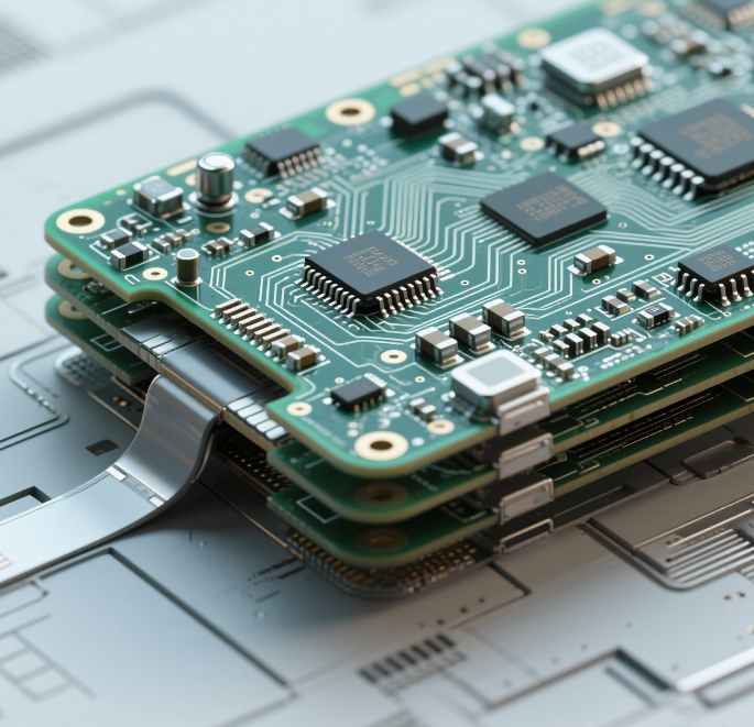
Ensuring Reliability and Longevity
reliability and longevity are critical, especially for applications in communication, AIoT, automotive, industrial control, and medical devices where failures can lead to system-wide consequences. To ensure long-term performance and minimal failure rates, manufacturers must implement best practices across design, material selection, assembly, and testing.
Key strategies include:
High-quality materials: Use of durable PCB substrates (e.g., FR4, polyimide, Rogers) and components rated for temperature, humidity, and vibration resistance.
Robust soldering processes: Precision reflow soldering, wave soldering, and selective soldering to avoid cold joints, voids, or bridging.
Conformal coating and encapsulation: Protection against moisture, dust, corrosion, and chemical exposure in harsh environments.
Thermal management: Heat sinks, thermal vias, and copper pours to prevent overheating in dense or high-power designs.
Design for Reliability (DfR): Inclusion of redundant traces, surge protection, and conservative current/voltage margins.
Environmental and stress testing: Thermal cycling, burn-in tests, vibration, ESD, and salt spray tests to simulate real-world conditions.
Traceability and process control: Full documentation of component batches, assembly conditions, and inspection data for quality assurance and warranty traceability.
By prioritizing these practices, PCB assembly providers can deliver products that perform reliably over extended lifespans, even in mission-critical or demanding operating conditions.
Conclusion
Communication and AIoT PCB Assembly represents the forefront of modern electronics manufacturing, where precision, performance, and adaptability converge. With the integration of advanced technologies such as HDI, flexible PCBs, AI chips, and 5G-ready materials, manufacturers are enabling the development of smarter, faster, and more compact devices. Customization and flexibility in assembly services further empower businesses to bring unique, application-specific products to market efficiently.
Equally important is the commitment to reliability and longevity, achieved through high-quality components, rigorous testing, robust process control, and thoughtful design. As the demand for intelligent and connected systems continues to rise, the ability to deliver innovative, scalable, and dependable PCB solutions will be key to staying competitive in the rapidly evolving landscape of AIoT and communication technologies.
Ready to Elevate Your PCB Projects to New Heights?
Whether you're developing next-generation communication devices or innovative AIoT solutions, we're here to turn your vision into reality. With advanced technologies, flexible manufacturing, and uncompromising quality standards, we deliver PCB assembly services that are smart, scalable, and built to last.
Contact us today to discuss your project needs and discover how our tailored solutions can accelerate your product development — from prototype to mass production.
Let's build the future, together.
New Energy and Automotive PCB Assembly
Understanding New Energy Vehicle (NEV) PCBs
New Energy Vehicles (NEVs), including electric vehicles (EVs), hybrid electric vehicles (HEVs), and fuel cell vehicles, rely heavily on specialized PCBs (Printed Circuit Boards) to support their advanced electronic systems. Unlike traditional vehicles, NEVs require high-reliability, high-power, and thermally optimized PCBs to ensure safe and efficient performance under demanding operating conditions.
Key Roles of PCBs in NEVs:
Battery Management Systems (BMS): Monitor and balance battery cells, track voltage, current, and temperature.
Power Conversion Systems: Support inverters, DC-DC converters, onboard chargers (OBCs), etc.
Motor Control Units (MCUs): Handle real-time motor operation and torque control.
Vehicle Control Units (VCUs): Centralized control of communication between subsystems.
ADAS and Infotainment Systems: Enable driver assistance, navigation, connectivity, and in-car experiences.
Key Features of NEV PCBs:
High Voltage and Current Tolerance: Required for handling battery packs, inverters, and power electronics.
Excellent Thermal Management: Use of thick copper layers, metal core PCBs (MCPCBs), and thermal vias.
Reliability under Harsh Conditions: Must withstand vibration, moisture, temperature extremes, and long operating cycles.
Compliance with Automotive Standards: Must meet stringent certifications such as IATF 16949, ISO 26262 (functional safety), and AEC-Q200.
NEV PCBs play a crucial role in ensuring vehicle safety, energy efficiency, and intelligent control. As the global shift toward electrification accelerates, demand for advanced, durable, and precisely assembled PCBs continues to grow — making them a backbone of the new energy automotive industry.
Key Components of New Energy Vehicles
New Energy Vehicles (NEVs)have someunique components that ensure efficient operation. Here are the key components:
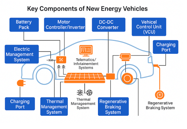
Main Power Control Systems in New Energy Vehicles
|
System |
Function / Description |
|
Battery Management System (BMS) |
Monitors and manages the health, charging, discharging, and temperature of the battery pack to ensure safe and efficient operation. |
|
Motor Controller / Inverter |
Converts DC from the battery into AC to drive the electric motor; controls speed, torque, and direction of the vehicle. |
|
Vehicle Control Unit (VCU) |
Serves as the “brain” of the powertrain; coordinates power delivery by managing the BMS, inverter, motor, and other subsystems. |
|
On-Board Charger (OBC) |
Converts external AC input into DC to charge the vehicle's battery; manages voltage regulation and charging profiles. |
|
DC-DC Converter |
Steps down high-voltage DC from the battery pack to lower-voltage DC for auxiliary systems (e.g., lighting, infotainment, ECU). |
|
Thermal Management System |
Maintains optimal temperatures for the battery, motor, and power electronics to ensure performance and extend lifespan. |
|
Energy Recovery System |
Manages regenerative braking, converting kinetic energy back into electrical energy for battery storage. |
Applications of New Energy Vehicle PCBs
Printed Circuit Boards (PCBs) in new energy vehicles are crucial for numerous applications. These boards control various electronic systems, ensuring the vehicle operates efficiently and safely. Here are some key applications of new energy vehicle PCBs:
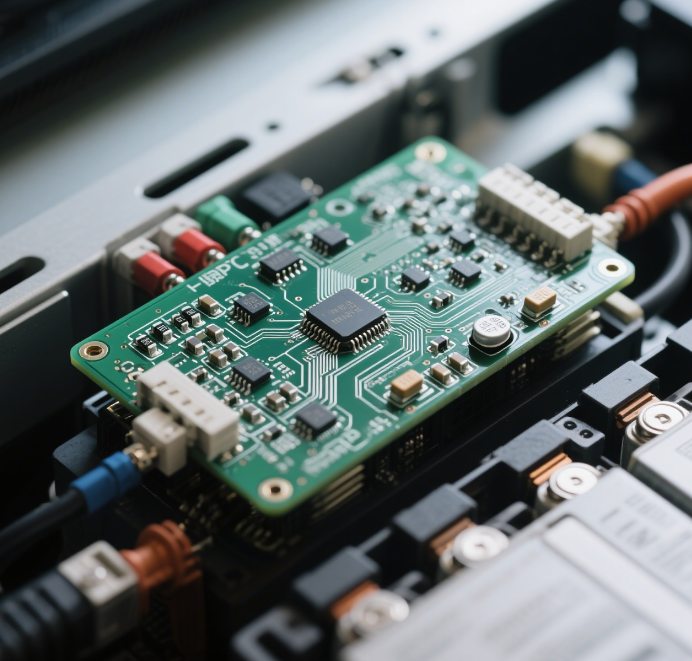
Unique Features of New Energy Vehicle PCBs
New energy vehicle PCBs are designed to meet the specific demands of electric vehicles. Here are their key features:
1. High Voltage and High Current Tolerance
NEV PCBs must handle high-voltage systems (typically 400V–800V for EVs).
Require thicker copper layers (up to 3oz or more) and wider traces to support high current flow, especially in battery management systems (BMS) and motor controllers.
2. Excellent Thermal Management
NEV power components generate significant heat.
Use of metal-core PCBs (MCPCBs), ceramic substrates, and thermal vias for efficient heat dissipation.
Integration with liquid cooling or heat sinks in critical zones.
3. High Reliability in Harsh Environments
Must endure extreme temperature fluctuations, moisture, vibration, and dust.
Require automotive-grade materials, conformal coating, and robust encapsulation.
4. High-Frequency and High-Speed Signal Capability
NEVs include advanced ADAS (Advanced Driver Assistance Systems), autonomous driving tech, and wireless communication modules.
PCBs often use high-frequency laminates (e.g., Rogers, Taconic) to support RF and millimeter-wave signals.
5. Multi-Layer and Rigid-Flex Designs
Need to accommodate dense, space-constrained layouts (e.g., in compact control units).
Use of multi-layer and rigid-flex PCBs to integrate signal, power, and control circuits in 3D formats.
6. Functional Integration
NEV PCBs integrate various systems like:
Battery Management System (BMS)
Inverter/Converter modules
Onboard Chargers (OBC)
Vehicle Control Units (VCU)
Emphasis on modular design and embedded components for efficiency and compactness.
7. Electromagnetic Compatibility (EMC)
EV power electronics generate significant electromagnetic noise.
PCBs are designed with EMI shielding, ground planes, filters, and optimized trace layout to reduce interference.
8. Strict Quality and Testing Standards
Must meet standards like IATF 16949, ISO 26262 (functional safety), and AEC-Q200 for electronic components.
Undergo in-circuit testing (ICT), functional testing (FCT), thermal cycling, X-ray, and environmental stress screening (ESS).
Materials and Technologies for New Energy Automotive PCB Assembly
The rapid evolution of new energy vehicles (NEVs) demands innovative materials and technologies in PCB assembly to meet higher performance, reliability, and efficiency standards.
Materials for New Energy Vehicle PCB Assembly
1. Base Substrate Materials
FR-4 (High-Tg & Halogen-free): Common but upgraded for better thermal stability.
Polyimide: Used in flex and rigid-flex PCBs for high heat resistance.
Metal Core (MCPCB): Aluminum or copper core for thermal conductivity, ideal for power modules.
Ceramic Substrates (AlN, Al₂O₃): Exceptional thermal performance and electrical insulation, often used in inverters and power control modules.
2. Copper Foil
Heavy Copper (≥2 oz/ft²): Supports high current flow; common in powertrain systems.
Embedded Copper Coin Technology: Improves heat dissipation and current carrying capacity.
3. Solder Mask and Surface Finish
High-temperature resistant solder masks: Withstand reflow cycles and operating heat.
ENIG (Electroless Nickel Immersion Gold): Preferred for fine-pitch and high-reliability.
OSP, ImAg, or ENEPIG: Alternative finishes, chosen based on assembly and cost needs.
4. Conformal Coatings
Protect PCBs from moisture, salt spray, chemicals, and vibration.
Common coatings: Acrylic, Polyurethane, Silicone, or Parylene.
Advanced Technologies in NEV PCB Assembly
1. High-Density Interconnect (HDI)
Allows compact design with fine pitch, used in BMS and control units.
Laser drilling, microvias, and sequential lamination enable advanced layering.
2. Embedded Components
Passive or active components embedded within the PCB.
Reduces size and increases reliability by minimizing interconnects.
3. Rigid-Flex Technology
Combines rigid and flexible PCBs in a single design.
Ideal for space-constrained modules like dashboard electronics or sensor units.
4. Selective Soldering and Reflow
Precise soldering techniques suited for mixed technology boards (SMD + THT).
Ensures thermal control during soldering of sensitive automotive-grade components.
5. Automated Optical and X-Ray Inspection (AOI / AXI)
Guarantees solder joint integrity, especially in BGA, LGA, and QFN packages.
AXI is essential for double-sided and high-layer boards.
6. Functional and In-Circuit Testing (FCT/ICT)
Ensures performance and safety compliance.
Often integrated with vehicle simulation environments for real-world testing.
7. Thermal Simulation and Reliability Modeling
Use of thermal simulation software (e.g., ANSYS, FloTHERM) in design phase.
Helps predict hot spots, failure points, and guides material selection.
Design and Prototyping Process for New Energy Vehicle PCBs
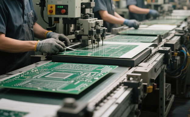
1. Requirements Analysis
Define system architecture (e.g., Battery Management System, Motor Control, Charging Module).
Analyze:
Voltage/current requirements
Thermal management needs
Space constraints
EMC compliance
Automotive safety standards (ISO 26262, AEC-Q200)
2. Schematic Design
Electrical design using CAD tools (e.g., Altium Designer, OrCAD).
Careful component selection with automotive-grade certifications.
Redundancy and fail-safe circuitry for critical systems (e.g., VCU or BMS).
3. PCB Stack-Up and Layer Planning
Choose appropriate layer count (often 6–12 layers or more for NEVs).
Plan for:
Power and ground plane separation
Signal integrity
Thermal via placement
High-current copper routing
4. PCB Layout Design
Precise component placement to minimize thermal and EMI issues.
Use differential pair routing and impedance control for high-speed signals.
Place thermal reliefs, heat sinks, or metal cores in high-power zones.
Incorporate test points, edge connectors, and mounting holes as needed.
5. Thermal and Signal Simulation
Use simulation tools like:
ANSYS, HyperLynx, or FloTHERM
Analyze:
Heat dissipation
Voltage drop
Signal integrity
EMC performance
Iterate design before prototype fabrication.
6. Gerber Generation and DFM Review
Generate Gerber, BOM, pick & place, and netlist files.
Conduct DFM (Design for Manufacturability) and DFT (Design for Testability) checks.
Validate with PCB fabricator and EMS provider.
7. Prototype Fabrication
Choose appropriate material: FR-4 High Tg, Polyimide, Aluminum Core, or Ceramic.
Manufacture a limited prototype batch (e.g., 5–20 pcs).
Utilize quick-turn PCB services for fast validation.
8. PCB Assembly (PCBA)
Use automated SMT assembly with automotive-grade solder paste.
Apply selective soldering, BGA reflow, and AOI/AXI inspection.
Apply conformal coating for protection if needed.
9. Testing and Validation
Perform:
In-Circuit Test (ICT)
Functional Test (FCT)
Power cycling and thermal shock
Environmental stress screening (ESS)
Simulate actual vehicle operation conditions.
10. Prototype Review and Iteration
Analyze test results and collect feedback.
Revise design to fix issues such as:
Overheating
Noise coupling
Component failure
Prepare for pilot production after successful validation.
Key Considerations
Compliance: Meet automotive regulations (IATF 16949, ISO 26262).
Documentation: Maintain thorough design logs, change records, and test results.
Traceability: Use barcode/QR code tracking for each prototype board.
Conclusion
As the automotive industry shifts toward electrification and intelligent mobility, New Energy Vehicle PCBs are becoming increasingly critical in enabling safe, efficient, and high-performance systems. From power control and battery management to autonomous driving and connectivity modules, the design and assembly of NEV PCBs demand advanced materials, robust technologies, and strict quality standards.
The integration of high-voltage tolerance, thermal management, compact multilayer structures, and automotive-grade reliability ensures these PCBs can withstand the rigorous demands of next-generation vehicles. By following a well-structured process—from initial design and simulation to prototyping and testing—manufacturers can accelerate innovation while meeting safety and regulatory requirements.
Embracing cutting-edge PCB technologies will not only improve the efficiency and longevity of NEVs but also drive the future of sustainable, intelligent transportation.
Ready to Elevate Your PCB Projects to New Heights?
Whether you're developing cutting-edge new energy vehicles, advanced AIoT systems, or high-reliability industrial electronics, partnering with a trusted PCB assembly expert can accelerate your innovation and ensure long-term success.
At every stage—from concept and prototyping to full-scale production—we bring:
- Precision Engineering
- Advanced Manufacturing Technologies
- Stringent Quality Control
- Scalable, Turnkey Solutions
Let us help you transform your ideas into high-performance, future-ready products.
Contact us today to discuss your project requirements and discover how we can support your next breakthrough.
Medical Electronics PCB Assembly
Introduction
Medical electronics PCB assembly refers to the specialized process of designing, assembling, and testing printed circuit boards used in medical devices and healthcare systems. These PCBs serve as the electronic backbone of equipment ranging from portable diagnostic tools to life-critical systems such as defibrillators, patient monitors, MRI machines, and implantable devices.
Because human health and safety are directly involved, medical PCB assemblies must adhere to the highest levels of precision, reliability, and regulatory compliance. This requires:
Use of biocompatible and medical-grade components
Strict adherence to standards like ISO 13485, IPC Class III, and FDA 21 CFR Part 820
Rigorous testing, traceability, and documentation
Medical PCBs are often built with multi-layer, high-density, and miniaturized designs, supporting functions such as real-time data processing, wireless communication, and sensor integration. They are essential for enabling advanced diagnostics, remote monitoring, robotic surgery, and next-generation medical technologies.
Importance of PCBs in Medical Electronics
Printed Circuit Boards (PCBs) are at the core of nearly all modern medical devices, playing a critical role in enabling precise diagnostics, real-time monitoring, and life-saving treatments. Their importance lies in the following key areas:
1. Core Component of Life-Critical Devices
PCBs form the functional foundation of equipment such as:
ECG/EKG monitors
Defibrillators
Infusion pumps
Imaging systems (CT, MRI, X-ray)
Portable diagnostic devices
Surgical instruments and implants
These systems rely on stable and uninterrupted PCB performance to ensure patient safety and accurate operation.
2. Miniaturization and Portability
Medical devices are becoming more compact and portable. PCBs enable:
High-density circuit integration in small form factors
Use in wearable and implantable devices
Lightweight, flexible design for homecare and point-of-care technologies
3. High Precision and Reliability
Medical electronics demand ultra-high reliability and zero-tolerance for failure, especially in critical care:
PCBs are designed and assembled under IPC Class III standards
Use of redundancy, fail-safe circuitry, and error-checking systems
4. Support for Advanced Functions
Modern PCBs integrate components for:
Data acquisition and signal processing
Wireless communication (Wi-Fi, Bluetooth, LoRa)
AI and IoT connectivity for remote diagnostics and monitoring
Sensor integration for patient vitals and real-time alerts
5. Regulatory and Quality Compliance
To be used in medical applications, PCBs must comply with:
ISO 13485 for medical device quality management
FDA regulations (21 CFR Part 820) for design controls
RoHS/REACH for environmental safety
In short, without reliable PCBs, medical electronics would not be able to deliver the performance, accuracy, and safety required in today’s healthcare environment.
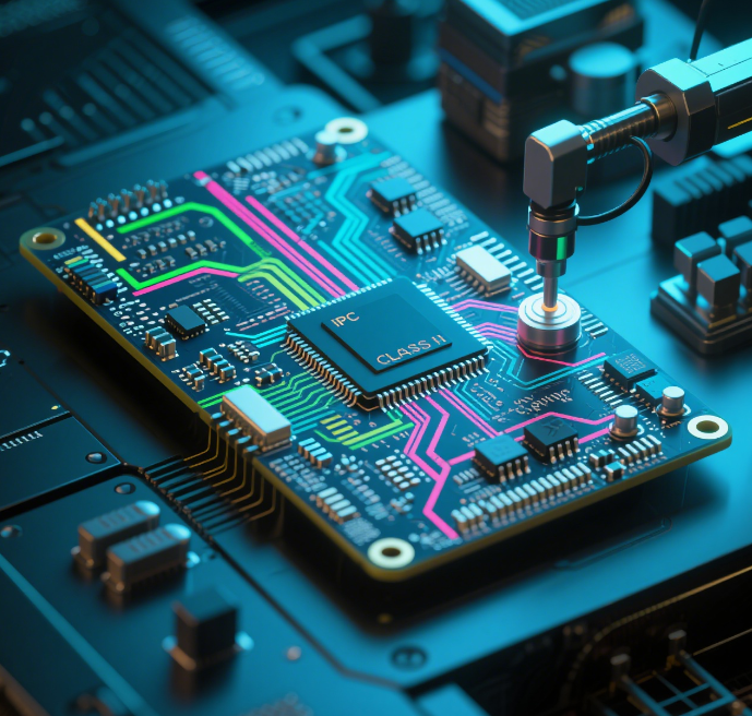
Benefits of Medical Electronics PCB Assembly
Medical electronics PCB assembly delivers the foundation for precision, safety, and innovation in today’s healthcare technologies. The benefits span across patient care, device performance, and regulatory compliance.
1. High Reliability and Safety
Medical PCBs are built to IPC Class III standards, ensuring the highest level of performance for life-critical devices.
Minimized risk of failure during operation in surgical, monitoring, and therapeutic applications.
Integration of redundant circuits and fail-safe designs for enhanced patient safety.
2. Support for Miniaturization
Enables compact and lightweight designs essential for:
Wearable health monitors
Implantable devices
Portable diagnostic tools
Facilitates multi-layer, rigid-flex, and HDI (High Density Interconnect) configurations.
3. Advanced Functional Integration
Supports real-time data acquisition, signal processing, and wireless transmission.
Allows integration of biosensors, microcontrollers, RF modules, and AI-capable chips.
Ideal for IoT-enabled medical systems and remote patient monitoring (RPM).
4. Strict Quality Assurance and Traceability
Assembled under cleanroom conditions with comprehensive testing (AOI, ICT, FCT).
Full component traceability, documentation, and lot control for regulatory audits.
Compliance with ISO 13485, FDA, RoHS, and UL standards.
5. Enhanced Patient Outcomes
Contributes to faster, more accurate diagnostics and improved treatment response.
Enables continuous monitoring and early detection of health risks.
Supports non-invasive, patient-friendly technologies.
6. Customization for Specialized Applications
Tailored PCB solutions for a wide range of medical fields:
Cardiology, neurology, radiology, emergency care, telemedicine, etc.
Flexible design options to meet unique form factors, power profiles, and biocompatibility needs.
Medical Electronics PCB Assembly is essential for advancing healthcare—delivering safe, smart, and scalable solutions for modern medical devices.
Challenges and Solutions in Medical Electronics PCB Assembly
The assembly of medical electronics PCBs presents unique challenges due to the life-critical nature, regulatory complexity, and miniaturization demands of medical devices. Addressing these challenges requires specialized knowledge, advanced technology, and rigorous process control.
1. Challenge: High Reliability and Zero Failure Tolerance
Issue:
Medical devices, especially life-support or surgical tools, must operate with near-zero failure rates. Even a single fault can pose a serious risk to patient safety.
Solution:
Follow IPC Class III standards for critical-use devices.
Use automotive/medical-grade components with extended life cycles.
Implement 100% AOI, X-ray, ICT, and FCT for thorough inspection and functional verification.
2. Challenge: Compliance with Stringent Medical Regulations
Issue:
Regulatory standards such as ISO 13485, FDA 21 CFR Part 820, and IEC 60601 require traceability, validation, and strict documentation.
Solution:
Establish a quality management system (QMS) that meets ISO 13485.
Maintain full component and process traceability.
Use validated manufacturing processes with documented DHR (Device History Records) and DHF (Device History Files).
3. Challenge: Miniaturization and Dense PCB Layouts
Issue:
Wearable, implantable, and handheld medical devices demand ultra-compact PCB designs with high component density, increasing risk of solder defects and layout constraints.
Solution:
Use HDI, microvia, and rigid-flex PCB designs.
Employ precision SMT machines for 01005 and BGA packages.
Utilize DFM and DFA analysis to optimize component placement and soldering quality.
4. Challenge: Thermal Management in Compact Designs
Issue:
Tightly packed electronics generate heat that may affect sensitive components or patient safety.
Solution:
Use high-Tg substrates, thermal vias, and metal-core PCBs (MCPCBs).
Integrate heat sinks or thermal interface materials (TIMs) in the design.
Perform thermal simulation during the design phase to predict hot spots.
5. Challenge: Biocompatibility and Patient Safety
Issue:
Some PCBs must be non-toxic, non-corrosive, and biocompatible, especially for contact or implantable devices.
Solution:
Choose biocompatible coatings (e.g., parylene) and materials.
Avoid harmful substances; ensure RoHS and REACH compliance.
Test materials for chemical resistance and long-term stability.
6. Challenge: Long Product Lifecycles and Component Obsolescence
Issue:
Medical devices often have 10–20 year lifespans, while components may be discontinued in a few years.
Solution:
Choose long-lifecycle or multi-source components.
Establish component lifecycle management and obsolescence strategies.
Collaborate with EMS providers offering supply chain continuity planning.
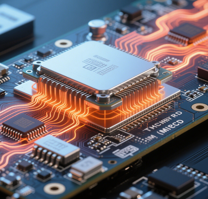
Medical electronics PCB assembly demands precision, quality, and accountability far beyond most other industries. By addressing challenges in reliability, regulatory compliance, thermal management, and design complexity, manufacturers can deliver safe, effective, and future-ready medical devices that improve lives and protect patients.
Conclusion
Medical electronics PCB assembly plays a crucial role in modern healthcare, forming the foundation for life-saving technologies, advanced diagnostics, and patient-centric innovations. Given the stringent reliability, safety, and regulatory demands, the design and assembly of medical PCBs require unmatched precision, process control, and industry expertise.
From wearable monitoring devices to complex imaging systems, success depends on high-quality PCB assembly that supports miniaturization, real-time data processing, wireless communication, and long-term reliability. By overcoming technical challenges and adhering to global standards such as ISO 13485, IPC Class III, and FDA 21 CFR, manufacturers can confidently deliver solutions that meet the evolving needs of healthcare professionals and patients alike.
As medical technology continues to evolve, investing in specialized PCB assembly ensures not just compliance—but also innovation, trust, and better health outcomes.
Ready to Elevate Your PCB Projects to New Heights?
When it comes to medical electronics, there’s no room for compromise. Whether you’re developing wearable diagnostics, surgical tools, imaging systems, or implantable devices, choosing the right PCB assembly partner is critical to achieving precision, reliability, and compliance.
We offer:
Expertise in medical-grade PCB design and assembly
Cleanroom assembly and advanced inspection systems (AOI, AXI, FCT)
Full traceability and ISO 13485/FDA-compliant processes
Custom solutions for low- and high-volume production runs
Let us help you bring your medical innovations to life with confidence and care.
Contact us today to discuss your project and explore how we can support your next breakthrough in healthcare technology.
Smart Home and Consumer Electronics Assembly
Key Components in Smart Home and Consumer Electronics PCB Assembly
Smart home and consumer electronics products are powered by compact, high-functionality PCBs that integrate a range of key components to deliver connectivity, automation, and user-friendly experiences. Below are the essential components commonly used in the PCB assembly process:
1. Microcontrollers (MCUs) / Microprocessors (MPUs)
Serve as the “brain” of the device, managing input/output, processing commands, and controlling other components.
Common in smart speakers, thermostats, remote controls, and home appliances.
2. Wireless Communication Modules
Enable devices to connect to Wi-Fi, Bluetooth, Zigbee, Z-Wave, or LoRa networks.
Essential for smart home devices like:
Smart bulbs and switches
Security cameras
Voice assistants
IoT hubs
Examples: ESP32, NRF52 series, CC3200, Zigbee SoCs.
3. Sensors
Detect changes in the environment and provide input to the system.
Types include:
Temperature & humidity sensors (e.g., DHT22, SHT31)
Motion/occupancy sensors (PIR, microwave, ToF)
Light sensors, gas sensors, and touch sensors
4. Display Interfaces
Provide visual feedback to users:
OLED or LCD screens for thermostats, smartwatches, and kitchen appliances
LED indicators for status notifications
Capacitive touch panels for seamless interaction
5. Power Management Components
Ensure stable power supply, voltage conversion, and battery charging.
Include:
Voltage regulators (LDO, buck/boost converters)
Power switches and MOSFETs
Battery charging ICs for portable electronics
6. Memory Chips
Store firmware, user settings, and data logs.
Common types:
Flash memory, EEPROM, SDRAM, and eMMC
Used in devices such as smart TVs, media players, and home hubs.
7. Audio and Video Processing ICs
Present in smart speakers, video doorbells, and smart cameras.
Include:
Audio codecs and amplifiers
Camera interfaces (CSI) and image signal processors (ISP)
8. Connectors and Interfaces
Ensure connectivity with other devices or peripherals.
Types:
USB (Type-C, Micro USB), HDMI, GPIO, antenna connectors
Spring-loaded connectors or edge connectors for docking systems
9. Actuators and Drivers
Control physical actions such as opening a lock, turning a motor, or adjusting volume.
Include:
Relay drivers
H-bridge motor drivers
Solenoid controllers
10. Protection and Filtering Components
Safeguard circuits from power surges, EMI, and static discharge.
Include:
ESD suppressors
Ferrite beads and EMI filters
Fuses and TVS diodes
Assembly Considerations
High-density SMT for compact designs
RoHS compliance for consumer safety
AOI and functional testing to ensure performance and reliability

The Smart Home and Consumer Electronics PCB Assembly Process
The assembly of PCBs for smart home and consumer electronics focuses on miniaturization, wireless integration, high-volume scalability, and cost-efficiency, while maintaining reliability and user safety. Below is a step-by-step breakdown of the typical process:
1. Design and BOM Preparation
Schematic capture and PCB layout using ECAD tools (e.g., Altium, Eagle)
Optimization for:
Compact design (often HDI or multilayer)
Wireless signal integrity (Wi-Fi, Bluetooth, Zigbee)
Generate:
Gerber files
Bill of Materials (BOM)
Pick & Place files
Assembly drawings
2. Component Procurement
Source components through authorized suppliers to ensure:
RoHS compliance
Proper ESD packaging
Availability for high-volume production
Emphasis on low-power ICs, wireless modules, and sensor integration
3. Solder Paste Printing
Apply solder paste to PCB pads using a stencil printer
High precision is critical for fine-pitch components like microcontrollers and RF chips
4. Pick and Place
Components such as MCUs, wireless modules, passives, LEDs, sensors, and connectors
Are placed onto the board using high-speed SMT machines
5. Reflow Soldering
Boards go through a multi-zone reflow oven
Solder paste melts and solidifies to create secure, reliable joints
6. Through-Hole Component Insertion (if applicable)
For devices with buttons, connectors, or large capacitors
Inserted manually or by automated insertion equipment
Followed by wave soldering or selective soldering
7. Inspection and Testing
AOI (Automated Optical Inspection):
Checks solder joints, part orientation, and placement
X-Ray Inspection (AXI):
For BGAs or hidden pads
ICT (In-Circuit Test):
Verifies component-level functionality and connectivity
FCT (Functional Circuit Test):
Simulates real-world usage to ensure performance
8. Programming and Calibration
Microcontrollers or SoCs are flashed with firmware
Device parameters are calibrated (e.g., sensor offsets, display alignment)
9. Conformal Coating (Optional)
Protects boards in humid or dusty environments, such as:
Smart thermostats, outdoor cameras, smart locks
10.Final Assembly and Packaging
Assembled PCBs are integrated into enclosures
Devices undergo burn-in, labeling, and final QA testing
Packaged with manuals, accessories, and ready for distribution
The smart home and consumer electronics PCB assembly process emphasizes:
High-speed wireless connectivity
Compact, modular designs
Rigorous testing and inspection
Scalability for mass production
With these steps, manufacturers can deliver innovative, user-friendly products that power the connected homes of tomorrow.
Benefits of Smart Home and Consumer Electronics PCB Assembly
Smart home and consumer electronics demand compact, intelligent, and connected devices. High-quality PCB assembly plays a critical role in delivering these expectations through efficient, scalable, and reliable electronics integration.
1. Miniaturization and Space Efficiency
Supports compact, lightweight designs for modern aesthetics and portability.
Enables integration of multi-layer, rigid-flex, or HDI (High-Density Interconnect) PCBs in slim enclosures (e.g., smartwatches, smart speakers).
2. Seamless Connectivity
Facilitates integration of wireless technologies like Wi-Fi, Bluetooth, Zigbee, and LoRa.
Powers smart devices such as home automation hubs, IoT sensors, and voice assistants.
3. Fast and Cost-Effective Production
Designed for mass production scalability using automated SMT assembly.
Reduces time-to-market for startups and established brands through quick-turn prototyping and efficient sourcing.
4. High Reliability and Quality Control
Modern PCB assembly lines use AOI, X-ray inspection, and functional testing (FCT) to ensure product quality.
Essential for preventing failures in devices like smart locks, home security cameras, and appliances.
5. Customizable and Flexible Design
Easily tailored to different product types and use cases:
From wearables to home entertainment systems
From simple sensor modules to multi-functional smart panels
6. Power Efficiency and Battery Optimization
Supports integration of low-power components and efficient power management ICs, enabling:
Long battery life in portable gadgets
Reduced energy consumption in always-on devices
7. Support for AI and Edge Computing
Accommodates MCUs, MPUs, and AI chips for real-time processing and automation.
Enables features like voice recognition, facial detection, and predictive control.
8. Enhanced User Experience
Facilitates sleek interfaces (touchscreens, voice control, LED feedback) and responsive performance, making devices more intuitive and user-friendly.
Smart home and consumer electronics PCB assembly empowers manufacturers to deliver connected, intelligent, and reliable products that meet the growing expectations of modern consumers. It forms the technological core behind smart living and digital lifestyles.

Applications and Use Cases
The demand for smarter, more connected lifestyles is driving the rapid adoption of PCB-based solutions in a wide range of smart home and consumer electronics devices. These applications rely on compact, reliable, and multifunctional PCB assemblies to power everything from automation to entertainment.
1. Smart Home Automation
Devices:
Smart light switches and dimmers
Smart plugs and outlets
Home automation control panels
Smart blinds and curtain controllers
Use Case:
Enables users to control lighting, power, and appliances remotely via smartphone or voice assistant, improving convenience and energy efficiency.
2. Voice-Controlled Devices
Devices:
Smart speakers (e.g., Alexa, Google Home)
Voice-enabled remote controls
Smart thermostats with voice support
Use Case:
PCBs integrate microphones, processors, and wireless modules to enable hands-free control and natural language interaction with smart ecosystems.
3. Home Security and Surveillance
Devices:
Wi-Fi cameras
Smart doorbells
Motion sensors
Smart locks and access control systems
Use Case:
Provide real-time video streaming, motion alerts, and remote access, enhancing both home security and peace of mind.
4. Environmental Monitoring
Devices:
Smart thermostats
Air quality monitors
Humidity and temperature sensors
Use Case:
Enable users to track and control indoor climate for better comfort, health, and energy savings—especially through automation and AI-based controls.
5. Wearable Consumer Devices
Devices:
Smartwatches
Fitness trackers
Smart rings and health monitors
Use Case:
Compact PCBs support Bluetooth connectivity, motion sensors, and battery optimization, making these devices lightweight, stylish, and powerful.
6. Home Entertainment Systems
Devices:
Smart TVs
Streaming boxes
Wireless soundbars and speakers
Gaming consoles and accessories
Use Case:
Provide HD audio/video processing, wireless streaming, and interactive experiences through high-performance PCB assemblies.
7. Smart Appliances
Devices:
Smart refrigerators, ovens, washing machines
Robotic vacuum cleaners
Coffee makers with app connectivity
Use Case:
Add connectivity, automation, and energy efficiency to traditional appliances using embedded PCBs with sensors and wireless chips.
8. DIY and Modular Smart Devices
Devices:
DIY smart kits (e.g., Arduino-based home control)
Customizable lighting systems
Modular IoT hubs
Use Case:
PCBs designed for plug-and-play functionality allow tech-savvy users and startups to prototype and scale new smart solutions easily.
From security and automation to wearables and entertainment, smart home and consumer electronics PCB assembly enables a connected, responsive, and intelligent living environment. The adaptability and scalability of these PCBs make them central to the evolving world of smart living.
Conclusion
Smart home and consumer electronics PCB assembly is at the heart of today’s digital lifestyle—enabling products that are smarter, smaller, and more connected than ever before. These assemblies support a wide range of applications, from home automation and security to wearables and entertainment systems.
With advancements in wireless integration, miniaturization, and mass production techniques, PCB assembly plays a vital role in transforming innovative ideas into high-performance, reliable, and user-friendly devices.
By leveraging modern PCB technologies and a reliable EMS partner, businesses can reduce time-to-market, enhance product quality, and meet the ever-growing expectations of tech-savvy consumers.
Ready to Elevate Your PCB Projects to New Heights?
At EdgePCBA, we’re not just experts in PCB assembly and fabrication; we're your partners in innovation and success.
Our commitment to quality, efficiency, and unparalleled customer service has supported countless projects across diverse industries, ensuring they meet their goals with the highest standards.
Don’t let PCB challenges slow you down. Whether you're in the military, medical, power, or commercial sectors, our seasoned team is here to provide tailored solutions that fit your unique needs.
From rapid prototyping to high-volume production, we have the expertise and capabilities to bring your ideas to life precisely and quickly.
We offer:
Expertise in compact, high-functionality PCB design and assembly
Scalable production for both startups and global brands
Fast prototyping, volume manufacturing, and flexible delivery
Advanced inspection, testing, and quality assurance
Let us help you bring your innovative ideas to life with speed, precision, and reliability.
Contact us today and let’s build the future of smart living—together.
Industrial Control Assembly
Introduction
Industrial control is assembly refers to the process of designing, assembling, and testing printed circuit boards (PCBs) and electronic modules used in industrial automation, machinery control, and intelligent manufacturing systems. These assemblies serve as the core controllers for equipment such as PLCs (Programmable Logic Controllers), HMIs (Human-Machine Interfaces), servo drivers, sensors, and robotics.
Unlike consumer electronics, industrial control systems require high reliability, long lifecycle, and resistance to harsh environments such as high temperatures, humidity, vibrations, and electrical noise. As such, the assembly process involves strict quality standards, ruggedized components, and compliance with industrial certifications (e.g., IPC-A-610, ISO 9001, UL, CE).
Industrial control assemblies play a vital role in enabling automated production lines, real-time monitoring, predictive maintenance, and IoT connectivity—paving the way for Industry 4.0 and smart factories.
Importance of PCBs in Industrial Control
Printed Circuit Boards (PCBs) are the backbone of industrial control systems, providing the electrical and structural platform for controlling, monitoring, and automating machinery and production processes. Their importance in industrial control lies in several key areas:
1. Centralized System Control
PCBs enable precise integration of microcontrollers, sensors, actuators, and communication interfaces into a compact, reliable unit. They are at the heart of devices like:
- Programmable Logic Controllers (PLCs)
- Motor and drive controllers
- Human-Machine Interfaces (HMIs)
- Industrial IoT gateways
2. High Reliability and Durability
Industrial environments are often harsh—characterized by high temperature, humidity, vibration, and electrical noise. PCBs used in these settings must:
- Withstand thermal cycling and mechanical stress
- Offer long-term performance with minimal failure
- Be made from industrial-grade materials with protective coatings
3. Real-Time Communication and Automation
PCBs support fast data processing and transmission between equipment, enabling:
- Real-time control and monitoring
- Process automation and safety interlocks
- Integration with SCADA and MES systems
4. Customization and Integration
Industrial control PCBs are often custom-designed to meet unique system requirements, allowing:
- Multi-functional integration (control + communication + power)
- Compact and efficient layouts
- Adaptability to different industrial protocols (e.g., Modbus, CAN, Ethernet/IP)
5. Support for Industry 4.0 and Smart Manufacturing
With the rise of smart factories, PCBs now incorporate features like:
- Wireless connectivity (Bluetooth, Wi-Fi, LoRa)
- Edge computing capabilities
- Data logging and AI-driven fault prediction
In summary, PCBs are indispensable in industrial control, enabling the transition to automated, intelligent, and connected manufacturing systems.
Benefits of Industrial Control PCB Assembly
Industrial control PCB assembly provides the foundation for intelligent, reliable, and scalable automation systems. Below are the key advantages:
1. High Reliability in Harsh Environments
- Built to withstand extreme temperatures, vibration, dust, and moisture.
- Uses industrial-grade materials, conformal coating, and reinforced designs to ensure long-term operation in challenging conditions.
2. Precision and Real-Time Control
- Enables accurate signal processing and fast response times for real-time system monitoring and control.
- Essential for applications like robotics, CNC machines, conveyor systems, and safety interlocks.
3. Customizable and Scalable Designs
- Tailored to meet specific industry requirements and equipment layouts.
- Easily scaled from prototype to mass production for use in everything from small control units to large automation systems.
4. Compact and Integrated Functionality
- Supports multi-functional integration: power management, signal control, and communication all on one board.
- Reduces the need for multiple separate modules, saving space, cost, and complexity.
5. Support for Smart Manufacturing
- Enables connection to industrial networks (e.g., Modbus, PROFINET, EtherCAT).
- Integrates with sensors, edge computing, and IoT platforms to support Industry 4.0 initiatives.
6. Enhanced Safety and Compliance
- Designs follow strict standards like IPC-A-610, UL, ISO 9001, and RoHS.
- Incorporates redundancy, isolation, and fail-safe mechanisms for enhanced operational safety.
7. Cost Efficiency Over Lifecycle
- Although built to higher specs, industrial PCBs reduce long-term costs by offering:
- Fewer maintenance issues
- Lower downtime
- Longer operational life
Processes and Standards in PCB Manufacturing and Assembly
1. PCB Manufacturing Process
a. Design and File Preparation
Create schematics and PCB layout in CAD software.
Generate Gerber files, BOM, and NC drill files.
Perform DFM (Design for Manufacturability) check.
b. Substrate and Copper Cladding
Use FR-4, polyimide, or metal-core materials.
Apply copper foil to create base layers.
c. Inner Layer Imaging and Etching
Print circuit patterns using photoresist.
Etch away unwanted copper to form traces.
d. Layer Lamination
Stack and laminate layers under high pressure and heat.
e. Drilling
Drill holes for vias, through-holes, and mounting using CNC machines or lasers.
f. Plating and Surface Finishing
Copper plating for vias and through-holes.
Surface finishes like ENIG, HASL, OSP, or ENEPIG applied.
g. Solder Mask & Silkscreen
Apply solder mask to protect traces.
Print silkscreen for labels and orientation markers.
h. Electrical Testing
Use flying probe or bed-of-nails testing to verify continuity and insulation resistance.
2. PCB Assembly (PCBA) Process
a. Solder Paste Printing
Apply solder paste to pads using a stainless-steel stencil.
b. Pick and Place
SMT machines place components onto the board at high speed and accuracy.
c. Reflow Soldering
Boards go through a reflow oven to melt solder and secure components.
d. Through-Hole Insertion (if any)
Components placed manually or with auto-insertion machines.
e. Wave or Selective Soldering
Used for THT components; selective soldering preferred for mixed-technology boards.
f. Automated Optical Inspection (AOI)
Detects misplaced components, solder defects, and polarity issues.
g. X-ray Inspection (AXI)
Used for BGA, QFN, and hidden solder joints.
h. Functional Testing (FCT) and In-Circuit Testing (ICT)
Verifies that the board functions correctly under simulated working conditions.
3. Key Standards and Certifications
Manufacturing Standards
IPC-A-600: Acceptability of printed boards.
IPC-6012: Qualification and performance of rigid PCBs.
IPC-2221: Generic PCB design standards.
Assembly and Quality Standards
IPC-A-610: Acceptability of electronic assemblies.
IPC-7711/7721: Rework, modification, and repair standards.
Automotive/Industrial Standards
ISO 9001: Quality management systems.
IATF 16949: Automotive quality management.
ISO 26262: Functional safety for road vehicles.
UL, RoHS, and REACH: Safety and environmental compliance.
Summary
Implementing these structured processes and adhering to recognized standards ensures:
High reliability and performance
Long lifecycle of PCBs in industrial environments
Compliance with safety and environmental regulations
Consistency across prototyping and mass production
Challenges and Solutions in Industrial Control PCB Assembly
Industrial control PCB assemblies must operate reliably in demanding environments. This brings specific challenges that require well-engineered solutions during design, manufacturing, and testing.
1. Challenge: Harsh Operating Environments
Issues:
High temperatures, humidity, dust, vibration, and electrical noise
Risk of corrosion, mechanical failure, or signal disruption
Solutions:
Use high-temperature resistant materials (e.g., High Tg FR-4, Polyimide)
Apply conformal coatings (e.g., silicone, acrylic, parylene)
Design with reinforced solder joints and vibration-resistant mounting
2. Challenge: Electromagnetic Interference (EMI)
Issues:
Signal degradation or malfunction due to noise from nearby equipment
Solutions:
Add EMI shielding, ground planes, and ferrite beads
Maintain proper trace spacing and routing
Use differential signaling and filtered connectors
3. Challenge: Complex Multi-Function Integration
Issues:
Need for combining control, communication, and power on one PCB
Risk of layout congestion and thermal accumulation
Solutions:
Use multi-layer and HDI (High-Density Interconnect) designs
Implement thermal vias, copper pours, and heat sinks
Leverage rigid-flex PCBs for space-constrained applications
4. Challenge: High Mix, Low Volume Production
Issues:
Industrial applications often require custom or semi-custom PCBs
Short production runs increase cost and complexity
Solutions:
Work with EMS providers offering flexible production lines
Use modular design approaches and DFM/DFT optimization
Adopt quick-turn prototyping and agile development cycles
5. Challenge: Ensuring Long-Term Reliability
Issues:
Industrial PCBs must function reliably over 10+ years
Solutions:
Use automotive/industrial-grade components
Perform aging simulations, thermal cycling, and ESS (Environmental Stress Screening)
Maintain rigorous traceability and documentation
6. Challenge: Strict Compliance and Certification
Issues:
Need to comply with standards like IPC-A-610, ISO 9001, CE, UL, and RoHS
Solutions:
Partner with certified manufacturing facilities
Integrate automated testing (AOI, ICT, FCT) and quality control at each stage
Ensure all components meet RoHS/REACH and industrial-grade specs
Conclusion
By addressing these challenges through robust design, precise process control, and advanced testing, manufacturers can ensure that industrial control PCB assemblies deliver exceptional performance and reliability—even in the toughest environments.
Conclusion
Industrial control PCB assembly is a cornerstone of modern automation and smart manufacturing. With growing demands for precision, reliability, and connectivity, PCBs used in industrial control systems must meet stringent standards and perform consistently in challenging environments.
From design and material selection to manufacturing, testing, and certification, every step plays a vital role in ensuring the long-term performance and safety of industrial equipment. By addressing the unique challenges of harsh conditions, EMI, and multi-functional integration, manufacturers can build robust solutions that power factories, infrastructure, and intelligent systems around the world.
In the age of Industry 4.0, investing in high-quality industrial control PCBs isn’t just a technical choice—it’s a strategic advantage for achieving efficiency, uptime, and competitive edge.
Ready to Elevate Your PCB Projects to New Heights?
At EdgePCBA, we’re not just experts in PCB assembly and fabrication; we're your partners in innovation and success.
Whether you're building advanced automation systems, high-reliability industrial controllers, or smart IoT-enabled machines, choosing the right PCB assembly partner is critical to your success.
We offer:
- Expertise in industrial-grade PCB design and assembly
- Strict compliance with international standards (IPC, ISO, UL, RoHS)
- Robust testing, inspection, and quality assurance
- Flexible, scalable manufacturing—from prototypes to mass production
Let us help you bring your industrial control solutions to life with precision, reliability, and speed.
Contact us today to start your next project with confidence.
Power Control PCB Assembly
Understanding Power Control PCB Assembly
Power Control PCB Assembly is at the heart of many electronic devices, ensuring they run smoothly and efficiently. It refers to the specialized process of designing and assembling printed circuit boards that manage, regulate, and distribute electrical power within electronic systems. These PCBs are critical in applications that involve high current, high voltage, or power conversion, such as industrial machinery, electric vehicles, power supplies, renewable energy systems, and motor drives.
What Is Power Control?
Power control involves:
Voltage conversion (AC-DC, DC-DC, etc.)
Current regulation and switching
Load distribution
Protection from overcurrent, overvoltage, and overheating
To accomplish these tasks, power control PCBs integrate specialized components and require robust materials and thermal management.
Key Features of Power Control PCB Assemblies
|
Feature |
Description |
|
High Current Traces |
Thick copper layers (2 oz or more) to handle large currents |
|
Thermal Management |
Metal-core PCBs (MCPCB), thermal vias, and heatsinks for heat dissipation |
|
Power Components |
MOSFETs, IGBTs, relays, transformers, power ICs |
|
Isolation and Safety |
Galvanic isolation, optocouplers, high-voltage spacing, conformal coating |
|
Durability |
High-Tg materials, flame-retardant laminates (e.g. FR4-TG170+), and robust solder joints |
|
Protection Circuits |
Fuses, TVS diodes, NTC thermistors, ESD protection devices |
Common Applications
Industrial Power Supplies
AC-DC converters, UPS, inverters
Electric Vehicles (EVs)
Battery management, motor controllers, onboard chargers
Solar and Wind Energy Systems
MPPT controllers, inverters, battery systems
Home Appliances
Power control for HVAC, washing machines, microwaves
LED Lighting Systems
High-efficiency drivers and dimmers
Assembly Considerations
Thick copper handling: Specialized etching and lamination process
Component spacing: Adequate clearance for high-voltage routing
Inspection: X-ray for through-hole power components and BGA packages
Testing: Hi-Pot test, burn-in, functional load testing under real operating conditions
Power Control PCB Assembly is essential for building reliable, safe, and efficient power electronics. It requires expertise in thermal management, high-power component handling, and stringent safety standards. A well-designed power control PCB not only ensures system stability but also extends the lifespan of the entire product.
Applications of Power Control PCB Assembly
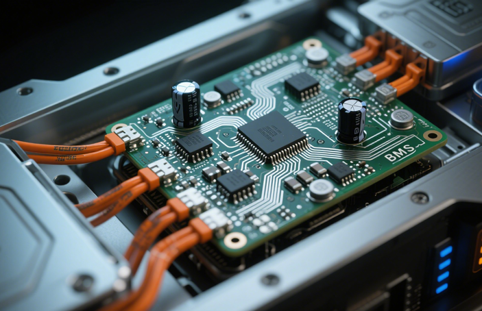
Power Control PCB Assemblies are essential in systems that require the conversion, regulation, and distribution of electrical power. These PCBs are designed to handle high current, high voltage, and heat dissipation, making them indispensable across multiple industries.
1. Electric Vehicles (EVs) and New Energy Vehicles
Applications:
Battery Management Systems (BMS)
On-board chargers (OBC)
Motor control units (MCU)
DC-DC converters and inverters
Purpose: Efficient power conversion, safe energy storage, and real-time control of traction systems.
2. Industrial Automation and Motor Control
Applications:
Programmable logic controllers (PLCs)
Servo drives and variable frequency drives (VFDs)
Industrial robots and CNC machines
Purpose: Precise motor control, load regulation, and automation of manufacturing processes.
3. Renewable Energy Systems
Applications:
Solar inverters and charge controllers
Wind turbine power conversion modules
Energy storage and hybrid power systems
Purpose: Converting and managing solar or wind power, ensuring grid compatibility and battery efficiency.
4. Power Supplies and UPS Systems
Applications:
AC-DC and DC-DC switching power supplies
Uninterruptible Power Supplies (UPS)
Power distribution units (PDUs)
Purpose: Provide stable, clean, and uninterrupted power for sensitive electronics and data centers.
5. Smart Home and Appliances
Applications:
HVAC power boards
Smart washing machines, refrigerators, and ovens
Power control for LED lighting systems
Purpose: Efficient energy usage and safe, reliable control in consumer devices.
6. Transportation and Rail Systems
Applications:
Traction control modules
Brake energy recovery systems
Power distribution in electric trains and metros
Purpose: Reliable power control under high-load and harsh conditions.
7. Telecom and Data Centers
Applications:
Power distribution for base stations
Rectifiers and power shelves in server racks
Backup and surge protection systems
Purpose: Continuous, fail-safe power to critical infrastructure.
8. Medical Equipment
Applications:
Power modules in imaging devices (MRI, CT)
Laboratory analyzers and sterilization equipment
Portable and backup medical power systems
Purpose: Stable, isolated power supply for patient safety and precision operation.
Power Control PCB Assemblies are a cornerstone in high-performance electronic systems. From electric vehicles to renewable energy and industrial automation, their role ensures efficient, safe, and reliable power handling in every application scenario.
Power Control PCB Assembly Process
The Power Control PCB Assembly Process encompasses several critical steps, each contributing to the creation of efficient and reliable electronic systems:
1,Design and Layout: Engineers design the PCB, outlining the circuit and component placement, focusing on efficiency, thermal management, and signal integrity. Read more about PCB Design and Basics.
2,Material Selection: Selection of appropriate materials for the PCB substrate and conductive layers to ensure durability under operational stresses. Materials commonly used in power control PCBS include FR-4, high-frequency laminates, and metal-core substrates.
3,Prototype Manufacturing: A prototype PCB is produced and tested to identify and rectify design issues before mass production.
4,Component Sourcing and Preparation: High-quality components compatible with the PCB design are sourced and prepared for assembly.
5,PCB Assembly: Components are attached to the PCB using Surface Mount Technology (SMT) for high-density designs or Through-Hole Technology (THT) for enhanced mechanical strength.
6,Inspection and Testing: The assembled PCB is inspected for defects and tested for functionality to ensure it meets all quality and performance standards.
7,Final Assembly: The PCB is integrated into its final assembly, including any necessary mechanical components and external interfaces.
8,Quality Assurance and Delivery: Final quality checks are performed before the power control system is packaged, documented, and shipped to ensure customer satisfaction.
Testing and Quality Assurance
Power control PCBs are deployed in high-stakes environments where failure can lead to system downtime, safety risks, or equipment damage. Therefore, rigorous testing and QA processes are essential to ensure electrical performance, thermal stability, and long-term reliability.
1. Automated Optical Inspection (AOI)
Detects:
Misaligned components
Solder bridging
Missing or reversed parts
Used after SMT assembly to ensure visual and placement accuracy
2. X-ray Inspection
Used for:
BGAs, QFNs, and power packages with hidden solder joints
Verifying voids, solder coverage, and internal lead connections
Critical for detecting failures invisible to AOI
3. In-Circuit Testing (ICT)
Validates:
Component values (resistance, capacitance)
Solder joint connectivity
Basic functional logic
Uses test probes or bed-of-nails fixture for high-speed, automated testing
4. Functional Testing (FCT)
Simulates real-world operating conditions
Confirms:
Voltage output regulation
Load switching performance
Short-circuit protection, overvoltage/undervoltage response
Often customized per customer specification or product design
5. Hi-Pot (High Potential) Testing
Applies high voltage across isolated sections (e.g., primary to secondary)
Verifies insulation integrity, isolation distances, and creepage compliance
Essential for power supplies and high-voltage modules
6. Burn-In Test (if applicable)
Runs the board under elevated voltage, current, and temperature for extended periods
Helps identify early-life failures and stress-sensitive components
Common in automotive, aerospace, and industrial power modules
7. Environmental & Reliability Tests (optional based on application):
Thermal cycling: Tests solder joint durability under rapid temperature shifts
Humidity and salt spray: For corrosion resistance
Vibration and shock testing: For rugged or mobile power modules
Conformal coating quality inspection: Ensures environmental protection layers are intact
Final Quality Assurance Checklist Includes:
Visual inspection (manual + machine)
Electrical performance verification
Labeling and traceability (serial numbers, barcodes)
Compliance with industry standards (IPC-A-610, UL, ISO, RoHS)
Testing and QA in Power Control PCB Assembly ensures that the board:
Performs safely under load
Withstands harsh operating conditions
Meets regulatory and customer standards
A strong QA process minimizes field failures and guarantees long-term system reliability in critical power applications.
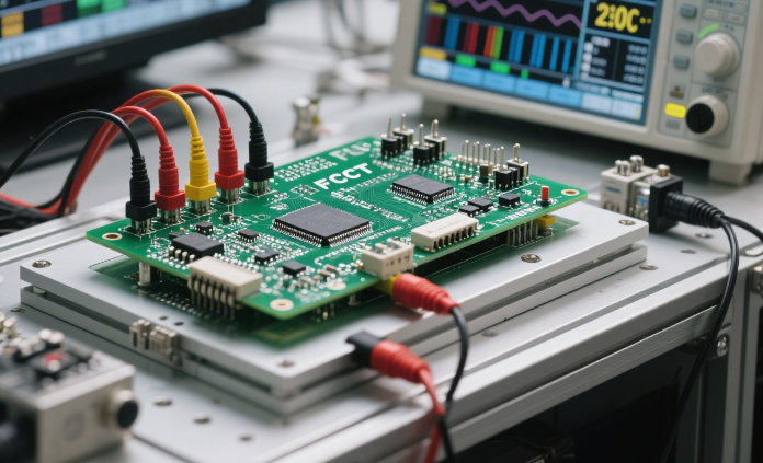
Benefits of Power Control PCB Assembly
Power Control PCB Assemblies offer numerous advantages that enhance the performance and reliability of electronic devices. Here are some key benefits:
Reliability
Reliability is paramount in any electronic device, and Power Control PCBs excel in this area. By using high-quality materials and rigorous testing processes, these assemblies ensure:
Consistent Performance: Devices operate smoothly without unexpected failures.
Long Lifespan: High reliability translates to a longer operational life for electronic devices.
Safety: Reliable PCBs minimize the risk of electrical failures that could lead to safety hazards.
Efficiency
Power Control PCBs are designed to manage and distribute power efficiently. This efficiency brings several benefits:
Reduced Energy Consumption: Efficient power management means devices use less energy, which is both cost-effective and environmentally friendly.
Optimized Performance: Devices perform better when they receive a stable and appropriate power supply.
Heat Management: Efficient PCBs help manage and dissipate heat, preventing overheating and maintaining performance.
Scalability
Scalability is a significant advantage of Power Control PCBs, allowing them to be used in various applications, from small gadgets to large industrial systems. Benefits include:
Customization: PCBs can be customized to meet the specific needs of different devices and applications.
Versatility: They suit various industries, including consumer electronics, industrial control, and renewable energy.
Future-Proofing: Scalable designs ensure that PCBs can accommodate future technological advancements and increased demands.
Durability
Durability ensures that Power Control PCBs can withstand harsh conditions and prolonged use. This is achieved through:
Robust Materials: Using high-quality, durable materials that can endure extreme conditions.
Protective Coatings: Apply coatings that protect against moisture, dust, and other environmental factors.
Mechanical Stability: Ensuring the PCB can handle physical stresses, such as vibrations and impacts.
Challenges in Power Control PCB Assembly
Designing and assembling Power Control PCBs come with a set of challenges that require innovative solutions:
Heat Management: Power control components generate significant heat. Efficient thermal management solutions are needed to dissipate this heat, preventing damage to the PCB and ensuring long-term reliability.
Space Constraints: As devices become smaller, integrating power control systems without compromising performance or safety becomes increasingly tricky.
Complexity and Cost: The need for high precision and reliability in Power Control PCB Assembly often leads to increased complexity and production costs.
Choosing the Right Power Control PCB Assembly Service
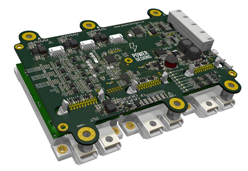
Selecting the right partner for Power Control PCB Assembly is critical, as these boards must meet high-performance, safety, and reliability standards. A qualified assembly service provider should offer technical expertise, process control, and industry compliance to support your project from design to delivery.
1. Experience in Power Electronics
Look for vendors with a proven track record in:
High-voltage and high-current applications
Power supply units (PSU), motor drives, EV systems, industrial controllers
Ask for reference projects or case studies in similar domains
2. Advanced Manufacturing Capabilities
Ensure they can handle:
Thick copper layers (2 oz to 6 oz or more)
Metal-core PCBs (MCPCB) or hybrid stack-ups
Large components, custom heat sinks, and high-power devices
Specialized wave soldering, selective solder, and SMT for heavy components are essential
3. Testing and Quality Assurance Systems
Confirm they offer:
Hi-Pot (high-potential) testing
Functional testing under load
Burn-in and reliability testing
AOI, X-ray inspection, and ICT should be standard
4. Standards and Certifications
Look for compliance with:
ISO 9001 – Quality Management
IPC-A-610 – Acceptability of Electronic Assemblies
UL, CE, RoHS, REACH – depending on your market
Automotive, medical, or industrial certifications as required (e.g. IATF 16949)
5. Design for Manufacturability (DFM) Support
Choose a partner who provides:
Design reviews to optimize trace width, spacing, and thermal layout
Stack-up guidance for high-current and EMI-sensitive designs
Recommendations for cost-efficient material selection and component sourcing
6. Supply Chain & BOM Management
Ensure robust procurement systems for:
Genuine power semiconductors (e.g., MOSFETs, IGBTs)
High-quality transformers, relays, connectors
Alternatives and lifecycle management for long-term product support
7. Customization and Flexibility
Look for assembly services that can handle:
Low to high-volume production runs
Custom packaging, conformal coating, or potting
Rapid prototyping and quick-turn delivery for urgent projects
8. Engineering & After-Sales Support
A reliable partner will offer:
Engineering consultation during the design phase
Clear communication throughout the project
Post-delivery technical assistance and warranty support
| Key Criteria | Why It Matters |
| Power assembly expertise | Ensures safety and performance |
| Thermal & current handling | Supports demanding applications |
| Full testing capabilities | Guarantees product reliability |
| Certifications | Ensures compliance with regulations |
| DFM + engineering support | Speeds up design and lowers costs |
| BOM + supply chain control | Prevents delays and counterfeit parts |
A Strategic Partner, Not Just a Vendor
The right power control PCB assembly service is more than a supplier — they’re a technical partner who helps bring your product to market faster, safer, and smarter.
Future Trends in Power Control PCB Assembly
As the demand for high-efficiency power systems, electrification, and intelligent control continues to rise, Power Control PCB Assembly is evolving rapidly. Emerging technologies, materials, and manufacturing methods are shaping the next generation of power electronics.
1. Higher Power Density Designs
Trend: Reducing board size while increasing power output
Impact:
Tighter layouts with thermal optimization
Integration of advanced cooling structures (e.g. embedded copper blocks, heat pipes)
Emphasis on compact, multilayer MCPCBs and hybrid stack-ups
2. Advanced Thermal Management
Trend: Heat is the biggest limiting factor in power PCB performance
Innovations:
Phase-change materials (PCM) and vapor chambers
Thermally conductive PCB substrates (ceramic, AlN, Si₃N₄)
Embedded thermal vias and active cooling modules
3. Wide Bandgap Semiconductors (SiC and GaN)
Trend: Shift from silicon to SiC (Silicon Carbide) and GaN (Gallium Nitride)
Benefits:
Higher switching frequencies
Better efficiency at high voltages
Requires PCBs with enhanced insulation, reduced parasitics, and lower EMI
4. Smart Power PCBs and Embedded Sensing
Trend: Integration of monitoring and control directly into PCBs
Features:
Embedded temperature, current, and voltage sensors
Real-time data feedback for predictive maintenance
Microcontroller or SoC integration for self-regulating power modules
5. Automated, High-Precision Assembly
Trend: Increased reliance on robotics and Industry 4.0 practices
Examples:
3D AOI and inline X-ray inspection
AI-assisted SMT placement and solder profiling
Digital twins for real-time manufacturing simulation
6. Electrification of Everything (EoE)
Trend: Electrification is extending to transportation, buildings, and industries
Effect:
Surge in demand for high-efficiency power conversion boards
More complex PCBs for EVs, energy storage systems, microgrids
7. Modular & Scalable Power Architectures
Trend: Standardized modular power PCBs for scalable integration
Use Case:
Swappable or stackable power modules
Faster time-to-market for OEMs
Simplified system maintenance and upgrades
8. Green Manufacturing & Sustainability
Trend: Growing focus on environmentally responsible production
Initiatives:
Lead-free, halogen-free materials
Low-carbon footprint PCB fabrication
Recyclable or biodegradable substrate development
| Trend Area | Key Direction |
| Power Density | Compact, multilayer thermal designs |
| Thermal Innovation | Active & passive advanced cooling |
| SiC/GaN Adoption | High-speed, high-voltage capabilities |
| Embedded Intelligence | Built-in sensors and control logic |
| Smart Manufacturing | Robotics, AI, real-time QA |
| Electrification Expansion | EVs, renewables, heavy industry |
| Modular Design | Scalable, pluggable power systems |
| Sustainability | Eco-friendly processes and materials |
The future of Power Control PCB Assembly lies in intelligent integration, material innovation, and digital precision. Businesses that adopt these trends early will lead the way in building safer, more efficient, and smarter power systems for tomorrow’s world.
Conclusion
The future of Power Control PCB Assembly looks promising, with ongoing advancements in materials and technologies. As devices become smaller and smarter, the demand for high-density, efficient, and reliable PCBs will continue to grow.
Integrating PCBs with IoT and other intelligent technologies will drive innovation, leading to more sophisticated and interconnected devices.
Power Control PCB Assemblies are the backbone of many modern electronic devices. For businesses and engineers looking to stay ahead in this competitive field, partnering with experienced and reputable PCB assembly services is crucial.
Ready to Elevate Your PCB Projects to New Heights?
Whether you're building high-performance power systems, intelligent control boards, or next-generation electronics, choosing the right PCB assembly partner is the key to success.
At EdgePCBA, we bring:
Proven expertise in Power Control PCB Assembly
Advanced capabilities in thermal design, high-current handling, and precision manufacturing
Rigorous testing, quality control, and compliance standards
Let us help you turn complex challenges into high-reliability solutions — from prototyping to mass production.
Contact us today to discover how we can empower your next breakthrough.
Request A Quote
Please feel free to contact us at any time, and we will wholeheartedly provide you with the highest quality service and support.